Executive Summary: Cool Designs for Hot Tech
Silicon Valley devices designers are adopting advanced thermal tests to optimize high-density printed circuit board (PCB) layouts. With the rise of high-power processors, compact consumer devices. And AI computing hardware, thermal management has become a key design step. By running thermal flow rules during the layout phase, designers can predict heat flow and eliminate hot spots before making begins. This virtual check reduces design cycles, prevents expensive board redesigns. And ensures long-term hardware safety.
As device devices get smaller, they become harder to cool. Today's designers pack chips, power regulators. And memory chips close together on tiny boards. Each of these parts generates heat during work. If the heat cannot escape, the heat of the board will rise rapidly. This can lead to thermal throttling, where the processor slows down to cool itself, or permanent hardware damage. Thermal test software helps designers solve this issue during the design phase.
The Physics of PCB Heat Dissipation
Managing heat on a circuit board requires a clear understanding of heat transfer. Circuit boards are made of fiberglass and copper layers. Fiberglass is a poor conductor of heat. Copper, on the other hand, is an excellent thermal conductor. Therefore, designers must use the copper layers of a PCB to guide heat away from hot chips and direct it toward cooling surfaces.
The primary method for moving heat through a board is the use of thermal vias. Thermal vias are small holes drilled through the board that are plated with copper. They connect the thermal pad under a hot chip to large copper planes on the inner or bottom layers of the board. This creates a low-resistance path for heat to flow through the board. From the bottom layer, the heat can be transferred to a metal heat sink or dissipated into the surrounding air through convection.
Designers also use thermal interface materials (TIMs), such as thermal paste or pads, to connect chips to heat sinks. Air is a poor conductor of heat. Even microscopically smooth metal surfaces have tiny air pockets between them. TIMs fill these gaps, replacing air with a highly conductive compound. This ensures quick heat transfer from the chip to the heat sink. This prevents hot spots and keeping the part running within safe limits.
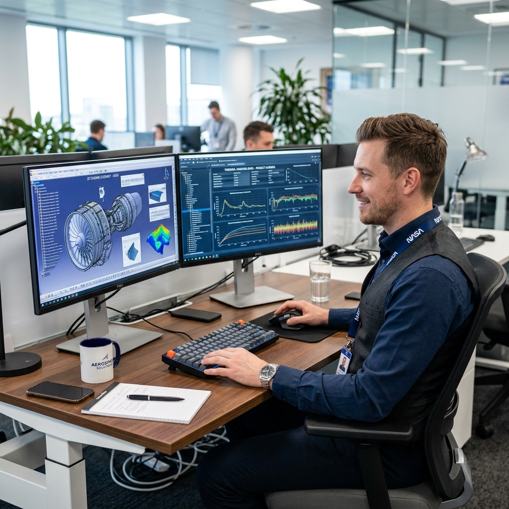
How Finite Element Analysis (FEA) and CFD Work
To model heat flow accurately, test software uses two main techniques: Finite Element Analysis (FEA) and Computational Fluid Dynamics (CFD). FEA is used to model heat conduction through solid objects. The software divides the CAD model of the PCB into a grid of tiny elements. It then solves equations to calculate how heat moves between adjacent elements, creating a detailed heat map of the board.
CFD is used to model how air or cooling liquids flow around the board. In a closed enclosure, air movement is key for carrying heat away. CFD software models the speed, heat. And path of air currents. It simulates how air enters the enclosure, moves across the parts. And leaves through exhaust vents. This helps designers place cooling fans, vents. And baffles in the best positions to maximize airflow and prevent stagnant, hot air pockets.
Running these tests requires significant computing power. High-density PCBs have hard copper traces and thousands of vias. Simulating every detail can take hours. To speed up the process, designers use cloud-based computing networks. This allows them to run multiple tests in parallel, comparing different part layouts and cooling designs in minutes. It enables an iterative design workflow where thermal feedback is integrated into the layout process.
Designing for Manufacturability and Cooling
Optimizing a PCB layout for thermal speed must be balanced with Design for Manufacturability (DFM). DFM ensures that a board can be fabricated and assembled easily and at a low cost. For example. Meanwhile, placing large copper pours around a hot part improves cooling, it can also make the board difficult to solder. The large copper mass acts as a heat sink during the soldering process, drawing heat away from the solder joint and creating cold solder joints. Cold solder joints are weak and can break easily.
To prevent this, designers use thermal relief pads. A thermal relief pad connects the part lead to the copper plane using narrow copper spokes rather than a solid connection. The narrow spokes restrict heat flow during soldering. This allows the joint to reach the correct heat. However, they still provide a path for heat to escape during device work. Finding the right balance between thermal speed and solderability is a key challenge for layout designers.
exact making is also key for thermal parts. Metal heat sinks and brackets must be made to tight tolerances. If a heat sink is slightly warped, it will not make flat contact with the chip, creating air gaps that block heat flow. U.S. Machine shops that support the tech sector use advanced CNC milling and turning to produce flat, smooth cooling parts. They often verify surface flatness using coordinate measuring machines (CMM) to ensure maximum thermal speed.
Why Thermal Optimization Matters for Tech Firms
For Silicon Valley tools companies, thermal test is essential for bringing products to market quickly. The tech trade is fast-paced. A delay of a few weeks can mean missing a market window. If a new hardware prototype fails its thermal tests, it can delay the project by months. The design team must modify the layout, build new prototypes. And repeat the tests. Simulating thermal speed digitally reduces the risk of late-stage design changes. This saves time and money.
Thermal optimization also improves product safety. High heat levels accelerate the aging of device parts. The safety of a silicon chip drops exponentially as its heat rises. By keeping parts cool, thermal design extends the lifespan of the device. This reduces warranty return costs and protects the company's brand reputation. It is a key factor for enterprise hardware, such as servers and network switches. This must run continuously for years without failure.
Finally, thermal test supports the design of green tools. Energy speed is a major focus for modern devices. When parts run hot, they consume more power and require larger cooling fans. By designing quick thermal paths, designers can reduce the energy needed to keep devices cool. This is particularly important for data centers, where cooling energy represents a significant portion of total operating costs.
Future Outlook: AI-Driven Thermal Design
Looking ahead, thermal test tools will become more robotic and integrated into the design workflow. Software developers are creating AI rules that can simply optimize part placement. The designer simply inputs the part list and thermal constraints. And the AI generates the optimal layout. This will eliminate the slow, manual trial-and-error process. This allows designers to design cool, reliable boards in a fraction of the time.
We will also see the rise of advanced cooling tools, such as vapor chambers and direct liquid cooling, in high-speed computing. Vapor chambers use a sealed flat tube filled with fluid to spread heat rapidly across a surface. Direct liquid cooling circulates coolant directly over the chips. Simulating these two-phase cooling tools requires advanced CFD tools. As AI workloads continue to grow, these high-end cooling methods will become rule in data centers and high-speed workstations.
For U.S. Devices makers, this evolution offers exciting opportunities. The demand for advanced computing hardware is driving investments in domestic packaging and build plants. Suppliers that combine high-quality SMT build, exact thermal part making. And advanced digital checks will be highly competitive. They will play a key role in supporting the next generation of technological new idea.
Frequently Asked Questions (FAQ)
Why do high-density PCBs require thermal test?
Answer: High-density PCBs package many device parts into a small space. These parts generate heat during work. If the heat is not dissipated, the heat will rise. This causes the parts to throttle or fail. Thermal test helps designers find and fix hot spots before the board is built.
What are thermal vias and how do they dissipate heat?
Answer: Thermal vias are small, copper-lined holes drilled through a circuit board. They connect hot parts on the top layer to large copper planes on the inner or bottom layers. This allows heat to flow through the board, using the copper as a pathway to escape into the air or a heat sink.
What is the difference between FEA and CFD in thermal design?
Answer: Finite Element Analysis (FEA) models how heat travels through solid parts, like metal brackets and circuit boards. Computational Fluid Dynamics (CFD) models how air or cooling liquids flow around the board to carry heat away. Designers use both to get a complete picture of cooling.
How does thermal optimization prevent hardware degradation?
Answer: Thermal optimization keeps device parts running within safe heat limits. Excessive heat speeds up liquid reactions that wear out silicon chips and solder joints. By keeping parts cool, thermal design prevents premature aging and failures, extending the hardware's life.
As devices shrink, managing heat becomes an layout problem; simulation allows us to optimize thermal paths before printing boards.