
What happened
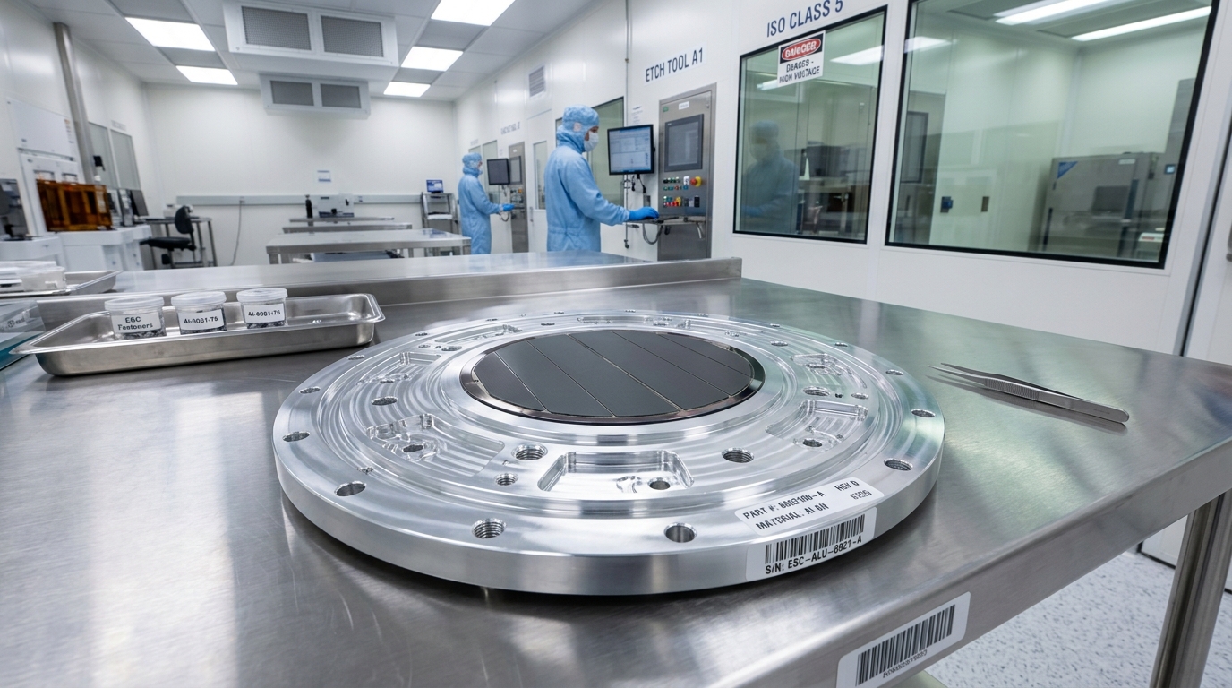
Illustration: RivCut
Semiconductor manufacturers with U.S. expansion plans are racing to hit a hard legislative deadline: construction must start by December 31, 2026 to qualify for the enhanced 35 percent Section 48D Advanced Manufacturing Investment Credit. As reported by Bloomberg, updated Treasury Department guidance issued in early August clarified exactly what counts as meeting that bar.
The stakes behind that clarification are significant. A modern leading-edge fab runs anywhere from several billion to well over ten billion dollars in total capital cost, and a 35 percent credit on that scale is not a rounding error on a balance sheet. It is often the difference between a project penciling out domestically versus at a competing site overseas, which is exactly the incentive the credit was designed to create when it was written into law.
The clarification matters because it resolved months of ambiguity. Preliminary site preparation and foundational concrete pours now qualify as a construction start, provided the fab operator has also signed equipment procurement contracts by year-end. That is a lower bar than a fully permitted, steel-in-the-ground groundbreaking, and it has triggered a wave of early procurement activity across Texas, Arizona, New York and Ohio as TSMC, Intel, Micron and Samsung move to lock in eligibility before the window closes.
Before this guidance, some fab operators were holding off on signing long-lead equipment contracts until they had a firmer legal read on what construction start actually meant, worried that spending on procurement without a qualifying physical start would not count toward the deadline at all. Treasury's clarification removed that ambiguity and effectively told the industry that tooling commitments made in good faith alongside site work will count, which is why the procurement activity accelerated so sharply in the days right after the guidance came out.
For each of these companies, the 35 percent credit on a multi-billion dollar fab is worth far more than the cost of accelerating a procurement timeline by a few months. That math is what is pulling equipment orders forward across the entire semiconductor tooling supply chain right now, four and a half months ahead of the deadline.
The states seeing the activity are not a coincidence either. Texas, Arizona, New York and Ohio already host established fab campuses with permitted land, existing utility infrastructure and a trained workforce nearby, all of which shorten the time between a signed contract and an actual concrete pour. A greenfield site in a state without that groundwork would struggle to hit a December 31 start date no matter how fast a company tried to move, which is part of why this deadline is concentrating investment in a handful of already-established manufacturing corridors rather than spreading it evenly across the country.
Why it matters for manufacturers
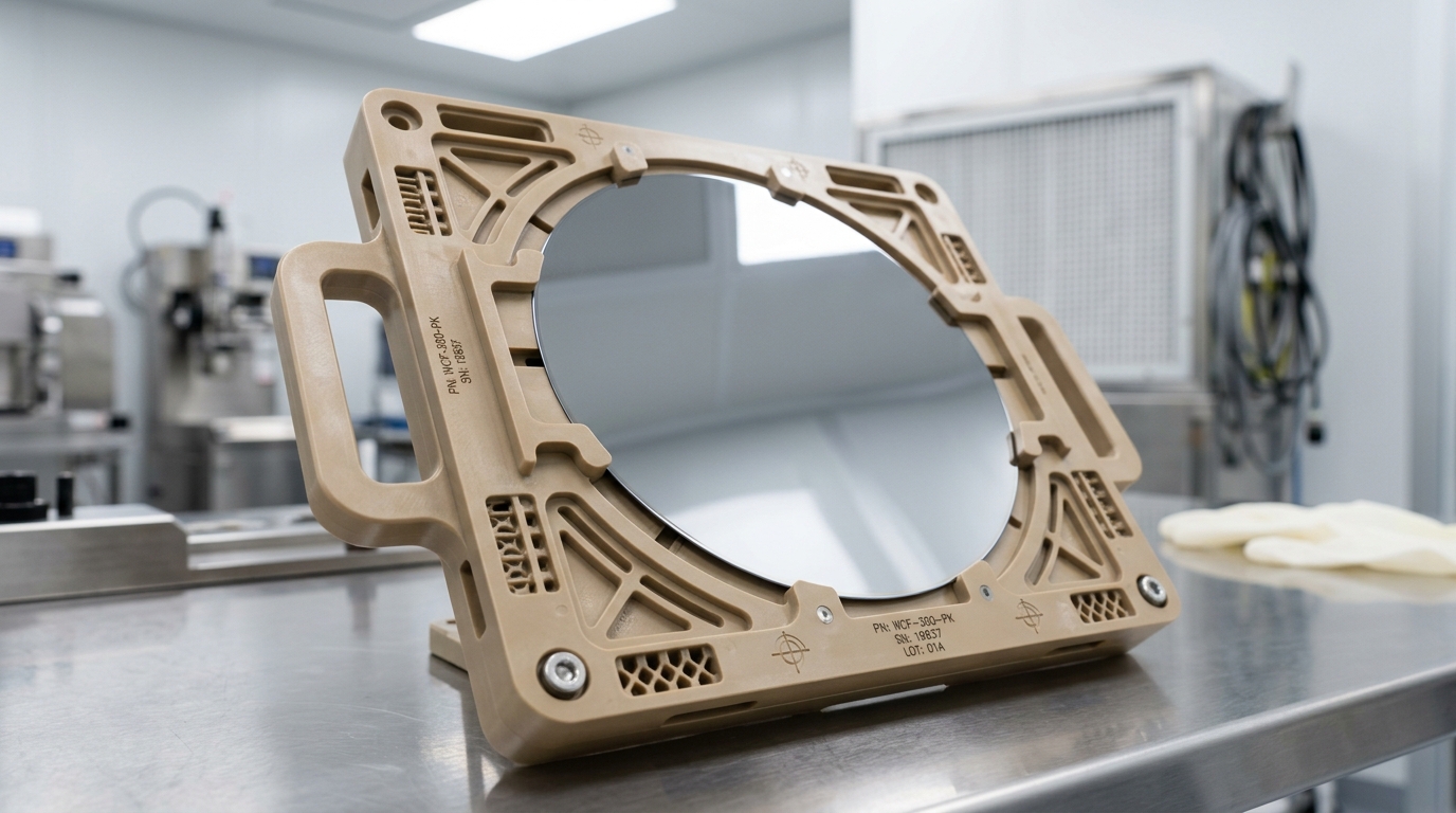
Illustration: RivCut
Semiconductor tolerances are a different category of hard
The rush to sign equipment contracts flows straight through to the precision machine shops that supply fab tooling, and this is not a market where a shop can simply add capacity by running more shifts. Semiconductor manufacturing equipment carries some of the tightest tolerance and finish requirements in the industry, routinely plus or minus 0.0001 inches with surface finishes at Ra 8 microinches or better. That level of precision demands thermally stable machine platforms, sub-micron metrology and operators who understand how a part's finish, not just its dimensions, determines whether it survives inside a vacuum chamber.
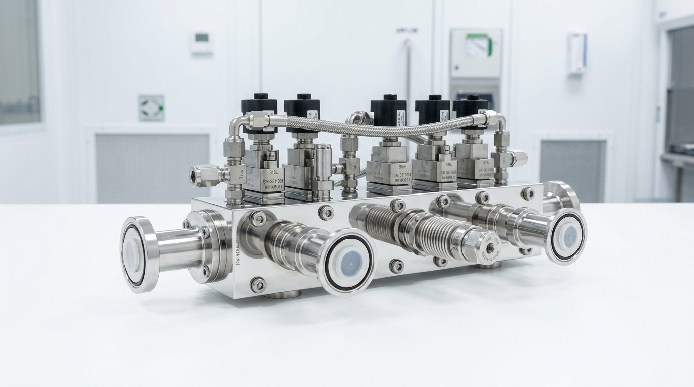
The components in highest demand right now are the ones every fab needs regardless of which chip it is building: high-purity aluminum gas distribution manifolds, electrostatic chuck baseplates, quartz wafer carriers, stainless steel vacuum chamber doors and chemical delivery valve blocks. Material selection is narrow and non-negotiable. 6061-T6 aluminum, 316L VIM/VAR stainless steel, Torlon, PEEK and high-purity ceramics are the standard palette, chosen because they hold dimensional stability and resist contamination inside a process chamber where a single stray particle can ruin a wafer lot.
Gas distribution manifolds illustrate why this work does not scale the way general machining does. Every internal port and channel has to be deburred and polished to a specification that leaves no trapped particulate behind, because a manifold delivering process gases into a chamber cannot introduce contamination that ends up embedded in a wafer. That polishing and inspection step often takes as long as the machining itself, which is why manifold lead times do not shrink proportionally just because a shop adds another 5-axis machine to the floor.
Electrostatic chuck baseplates carry their own version of this problem. The baseplate holds a wafer flat and thermally uniform during processing, which means its surface flatness has to be controlled to within a few microns across the entire diameter, not just at a handful of inspection points. A baseplate that is flat everywhere except one small region can still cause an uneven etch or deposition result across that wafer, so the inspection burden on a part like this is proportionally much larger than its size would suggest. Shops bidding on this work need metrology equipment, not just machining equipment, to compete credibly.
Cleanroom handling is its own discipline
Machining the part correctly is only half the job. Components headed for etch, deposition or photolithography tools have to be cleaned to ultra-high vacuum standards, inspected for particulates and double-vacuum packaged before they ever leave the shop floor. A machine shop can hold a perfect tolerance and still fail a fab's incoming inspection if its cleaning and packaging process introduces contamination after the fact. That is a capability most general-purpose contract shops simply do not have, which is why the shops that do have it are seeing order backlogs stretch out even as new capacity comes online elsewhere.
Standing up that capability from nothing is not a fast process either. A cleanroom-adjacent finishing area requires controlled airflow, particulate monitoring and staff trained specifically in contamination-free handling, none of which can be bolted onto an existing shop floor overnight. Fab operators know this, which is part of why they are locking in relationships with qualified suppliers now rather than waiting until equipment installation actually begins in 2027. By then, the shops with real cleanroom capacity will already be booked.
What to watch next
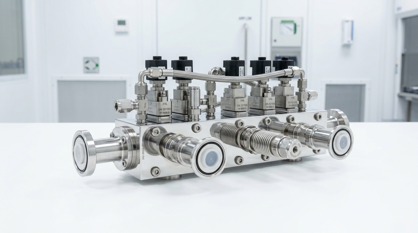
Illustration: RivCut
Through the rest of 2026, expect semiconductor capital equipment suppliers to push secondary subcontracts down to smaller specialty shops for structural frames, vacuum chambers and fluid control manifolds, as the prime toolmakers themselves hit capacity limits trying to serve every fab racing the same deadline.
Machine shops that already carry ISO 9001 and ISO 13485 cleanroom quality management certification are the ones best positioned to win multi-year supply agreements as this build-out shifts from groundbreaking activity into the tool installation phase through 2027. That transition, from pouring foundations to installing process equipment, is typically where semiconductor-adjacent machining demand peaks. Shops without cleanroom-qualified processes now will find the door largely closed by the time that phase arrives.
It is also worth tracking whether Treasury issues further guidance narrowing what qualifies as a legitimate construction start, since the current definition, preliminary site work plus signed equipment contracts, is broader than a traditional groundbreaking. If regulators tighten that definition later in the year to prevent companies from gaming the deadline with minimal site work, some projects currently counting on the credit could find their eligibility challenged after the fact. Fab operators moving fastest right now are the ones treating the current guidance as the floor, not the ceiling, and building a genuine construction record rather than the minimum required paperwork.
The rush to hit the tax credit deadline is straining high-purity semiconductor machine shops.