What happened
Micron Technology announced a collaboration with MetAI to build simulation-ready digital twins of semiconductor fabrication facilities using NVIDIA Omniverse, according to a June 3 release on PR Newswire. The partnership uses MetAI's MetGen platform to convert fragmented engineering data—CAD files, infrastructure specs, process documentation—into structured virtual models that comply with OpenUSD, the open-source Universal Scene Description standard Pixar originally developed for film production.
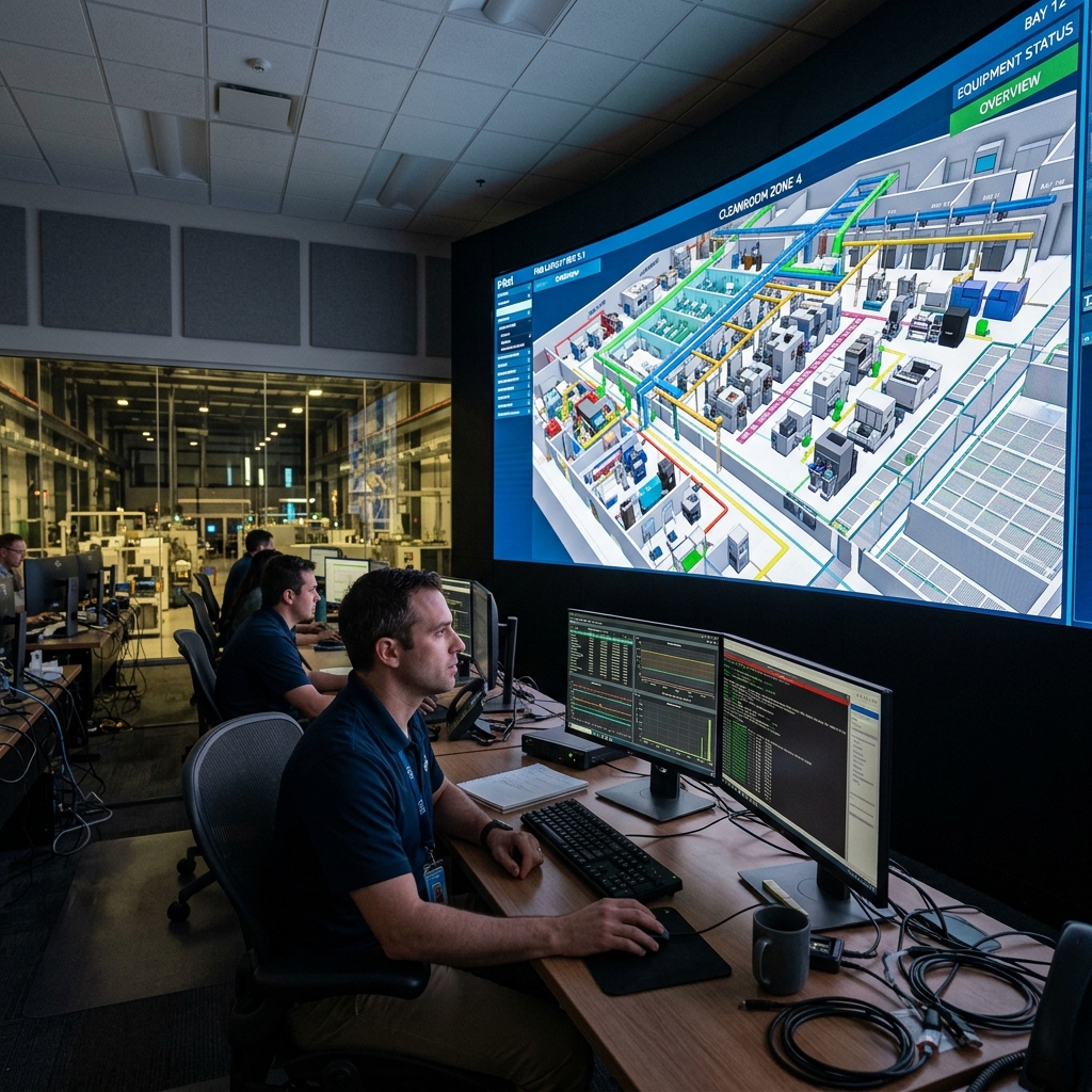
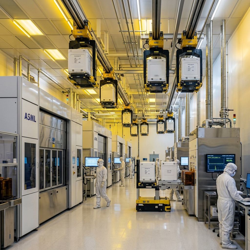
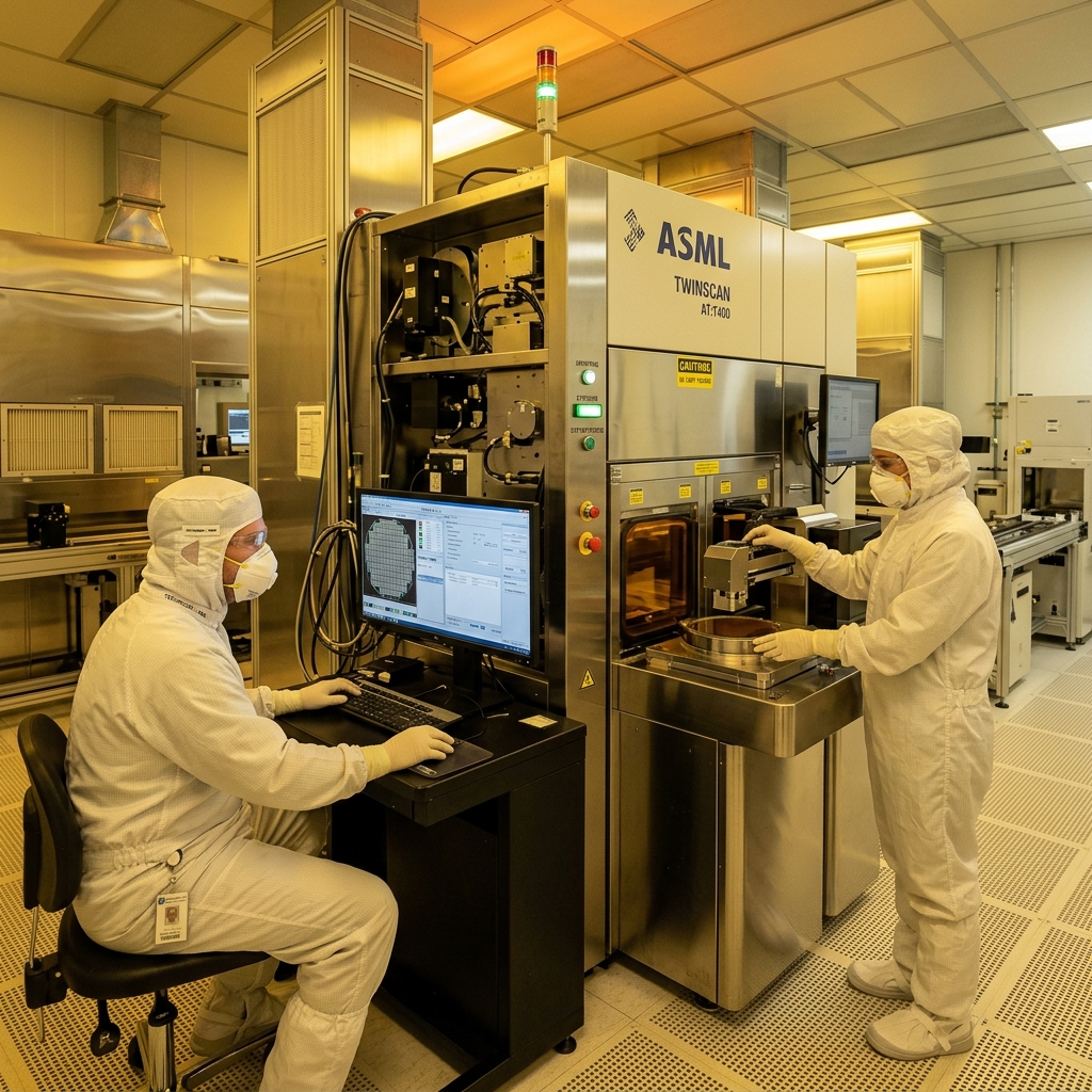
The digital twins simulate material flow, cleanroom layouts, and physical processes inside fabrication plants. NVIDIA Isaac Sim, a robotics simulation toolkit, connects to the models to train autonomous mobile robots and factory automation systems in a closed loop. Engineers can test equipment placements, workflow sequences, and logistics paths digitally before installing hardware or training human operators on the floor.
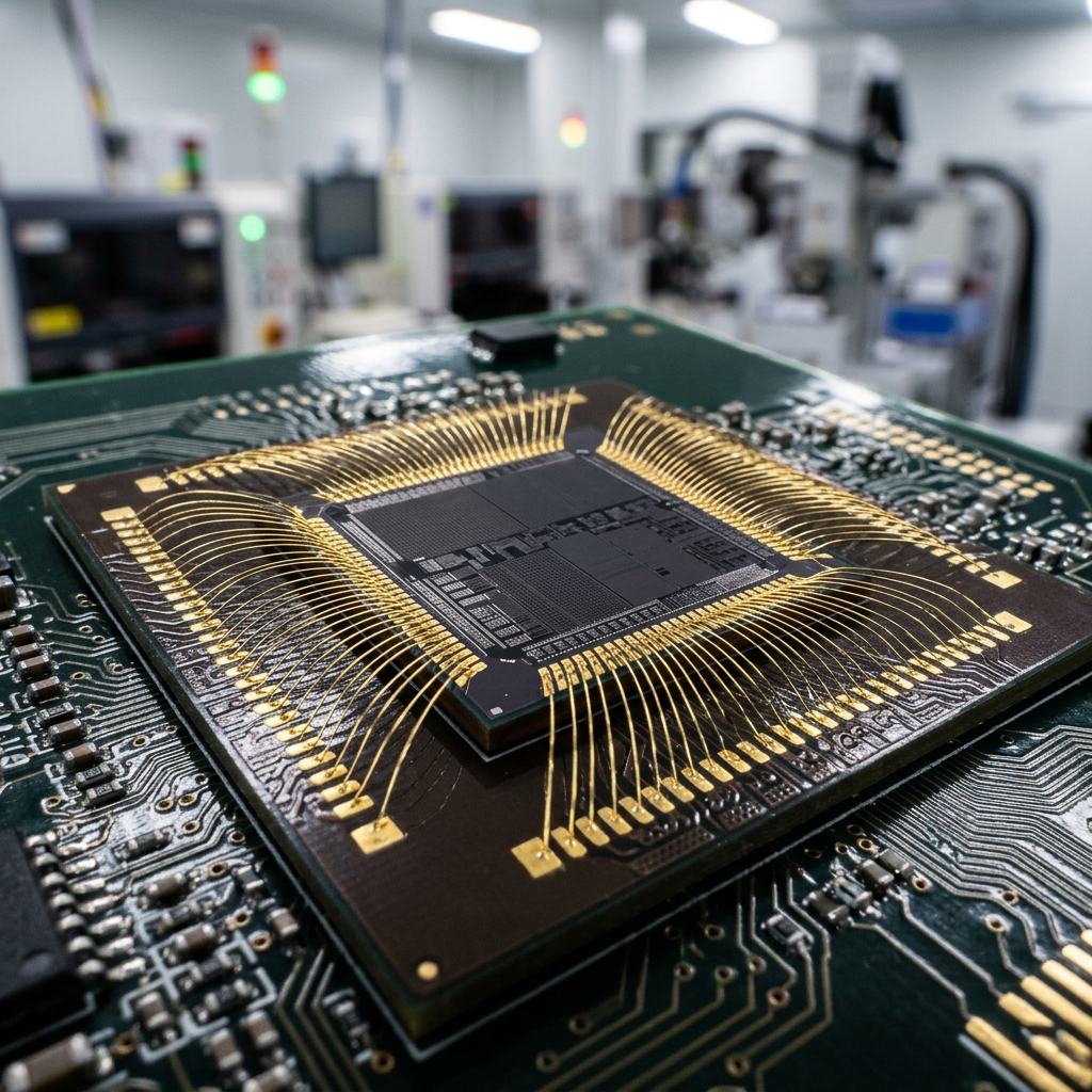
Micron operates fabs in Boise, Idaho; Manassas, Virginia; and Singapore, among other locations. The company manufactures DRAM and NAND flash memory, components with fabrication processes that require Class 1 and Class 10 cleanrooms where even minor layout inefficiencies translate to measurable yield loss. MetAI's platform aggregates data from multiple engineering disciplines—mechanical, electrical, process—that typically live in separate systems and formats.
The scale of Micron's construction plans is massive. They are spending up to $100 billion to build new mega-fabs in Boise, Idaho, and Clay, New York. Designing these plants is incredibly complex. Thousands of pipes must carry gases and chemicals to the tools. Power lines must supply high voltage. MetAI's MetGen software uses AI to clean up this data. Often, different vendors provide models in incompatible formats. Stitching them together by hand is slow and can lead to mistakes. MetGen automates this process, making the digital twin ready in days instead of weeks.
Once the model is ready, engineers can walk through it in virtual reality. They can check if maintenance access is clear. They can see if pipes interfere with other equipment. The virtual simulation also allows them to test different layout options. For example, they can compare a linear layout of lithography tools with a clustered layout. This helps them find the most efficient path for moving silicon wafers. Saving even a few seconds of travel time per wafer can increase the fab's output and save millions of dollars over the plant's lifetime.
Why it matters for manufacturers
Semiconductor fabs cost between eight and twenty billion dollars to build, and commissioning timelines stretch twelve to eighteen months after construction. A layout mistake discovered during equipment installation can idle entire toolsets while engineers reroute utilities or reconfigure clean corridors. Testing those decisions in software months earlier reduces the probability of expensive mid-build redesigns.
The approach also addresses a constraint that affects suppliers to the semiconductor industry. Cleanroom equipment, precision machined components, and metrology fixtures often arrive on site with lead times measured in quarters. If a digital twin flags a clearance problem or a workflow bottleneck during simulation, procurement can adjust orders before cutting metal or scheduling CMM inspection runs. That visibility matters when a single ion implanter occupies four hundred square feet of cleanroom real estate and requires custom-machined process chambers with tolerances under five microns.
Training factory robots in a virtual environment before deployment is not new—automotive manufacturers have used offline programming for decades—but applying the technique to semiconductor fabs introduces complications. Cleanrooms prohibit many materials, restrict airflow patterns, and demand particle counts below one per cubic meter in critical zones. A robot path that works on paper might generate unacceptable turbulence near a photolithography stepper or block access to a maintenance panel. Simulating those interactions in Isaac Sim lets engineers iterate on robot behavior without contaminating an actual cleanroom or halting production to test alternate routes.
The OpenUSD format is significant because it allows different simulation tools to share the same base model. An engineer running a computational fluid dynamics analysis to check airflow can work from the same digital twin a robotics team uses to program material handlers. That interoperability reduces the duplicated effort and version control problems that plague large capital projects.
Airflow management is one of the most critical aspects of cleanroom design. Fabs use vertical laminar flow systems. HEPA filters in the ceiling push clean air straight down to the floor. This carries dust particles away from the sensitive silicon wafers. If a robotic vehicle or a tool creates air turbulence, dust can swirl back up and land on the wafers. This ruins the chips. By simulating airflow inside the digital twin, engineers can adjust tool positions to prevent turbulence. RivCut specializes in machining wafer-handling components and vacuum chambers, and we know how critical cleanliness is for these parts.
This virtual testing also helps with tooling setup. Fabs use automated overhead transport (OHT) systems to move wafer pods. These are robotic vehicles that ride on tracks suspended from the ceiling. Setting up the OHT tracks is difficult because they must navigate around piping and electrical ducts. In the digital twin, engineers can run simulations of the OHT system. They can check for traffic jams or mechanical collisions. This ensures the physical tracks are installed correctly the first time, preventing delays during startup.
What to watch next
Micron's announcement does not specify which fab projects will use the digital twin workflow first, nor does it detail how much commissioning time the company expects to save. Those benchmarks will determine whether other chipmakers adopt similar approaches or treat this as a pilot limited to greenfield projects where engineering data starts in modern formats.
The broader question is whether the semiconductor supply chain will standardize on OpenUSD for equipment and facility data. If toolmakers and construction firms begin delivering models in that format, the aggregation work MetAI's platform handles today becomes less necessary. If they don't, fab operators will continue paying integration costs to stitch together incompatible datasets.
Procurement teams should also consider how virtual commissioning might shift lead time expectations. If a customer can validate a fixture design in simulation before ordering the physical part, tolerance negotiations and design review cycles could compress. That benefits suppliers who maintain digital libraries of standard components but disadvantages shops that rely on multi-week quoting processes to differentiate on engineering support.
For now, the Micron-MetAI collaboration signals that at least one Tier 1 chipmaker believes the cost of building and maintaining fab digital twins justifies the expense. Whether that calculation holds for smaller fabs, or for industries outside semiconductors with similar cleanroom requirements—pharmaceuticals, aerospace composites—remains an open question. More details at RivCut's semiconductor coverage.
We should also watch the "sim-to-real gap" in robotics. Isaac Sim uses advanced physics engines to simulate the cleanroom. But physical robots can still behave differently in the real world. For example, a robot might slip on a shiny cleanroom floor, or sensor noise might cause it to stop unexpectedly. If the simulation data does not transfer perfectly, engineers will still have to spend weeks tuning the robots on site. Watch if Micron reports high success rates for deploying virtual-trained robots directly to the cleanroom floor.
Lastly, pay attention to the security of these digital twins. Fabs are high-value targets for corporate espionage and cyberattacks. A digital twin contains the exact layout and process recipe of the factory. If hackers gain access to the model, they could steal valuable intellectual property or find vulnerabilities to exploit. Micron and its partners must build strong security measures to protect these virtual environments. Sourcing teams must also ensure that the data they share with the digital twin remains encrypted and secure.
Frequently Asked Questions
What is a digital twin of a semiconductor fab?
A digital twin is a highly detailed, virtual replica of a physical factory. In semiconductor manufacturing, it models the layout of the cleanroom, the placement of chemical piping, and the movement of robotic transport systems in real time.
Why are Micron and MetAI using the NVIDIA Omniverse platform?
They are using NVIDIA Omniverse to run simulations in a virtual environment. The platform allows engineers from different disciplines to test equipment placements, optimize workflow sequences, and train autonomous robots before the physical factory is built.
What is OpenUSD and why is it important for manufacturing?
OpenUSD (Universal Scene Description) is an open-source format for 3D data. It is important because it allows different engineering and design software programs to share the same virtual model, reducing errors and saving time during complex construction projects.
How does virtual simulation help prevent costly cleanroom design errors?
Cleanrooms cost billions to build and are highly sensitive to dust and airflow. A design mistake, like placing a machine where it blocks clean airflow, can ruin chip production. Virtual simulation catches these errors early, avoiding the need for expensive rebuilding.
Testing fab layouts in software months earlier reduces the odds of billion-dollar mid-build redesigns.