What happened
The Department of Commerce announced a $45 million CHIPS Act grant to expand advanced semiconductor packaging capacity in the Phoenix metro area. The funding will build new cleanrooms and purchase high-precision assembly equipment. These systems are dedicated to stacking and packaging multi-die processors, which is a key technology for artificial intelligence (AI) and high-performance computing. This investment aims to build a complete domestic semiconductor supply chain, ensuring that chips fabricated in the United States can also be packaged locally without relying on overseas facilities.
While the U.S. has made progress in reshoring wafer fabrication, advanced packaging remains heavily concentrated in Asia. This geographical mismatch has created a major vulnerability. Wafers processed in American fabs must still be shipped overseas to be sliced and packaged before they can be used in finished electronic products. The new Arizona facility aims to close this gap. By establishing a domestic packaging hub, the U.S. can protect its supply chain from shipping bottlenecks and trade disputes, ensuring that critical microprocessors remain secure and available.
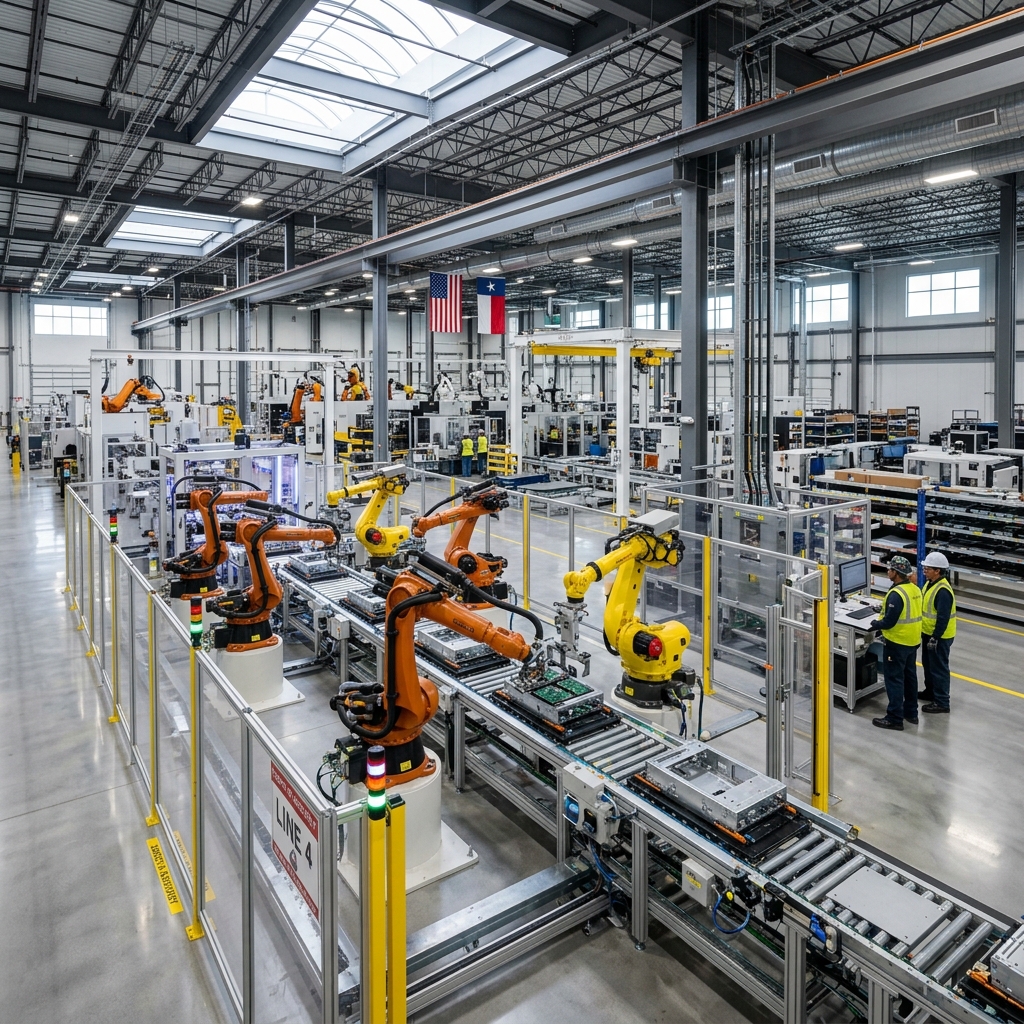
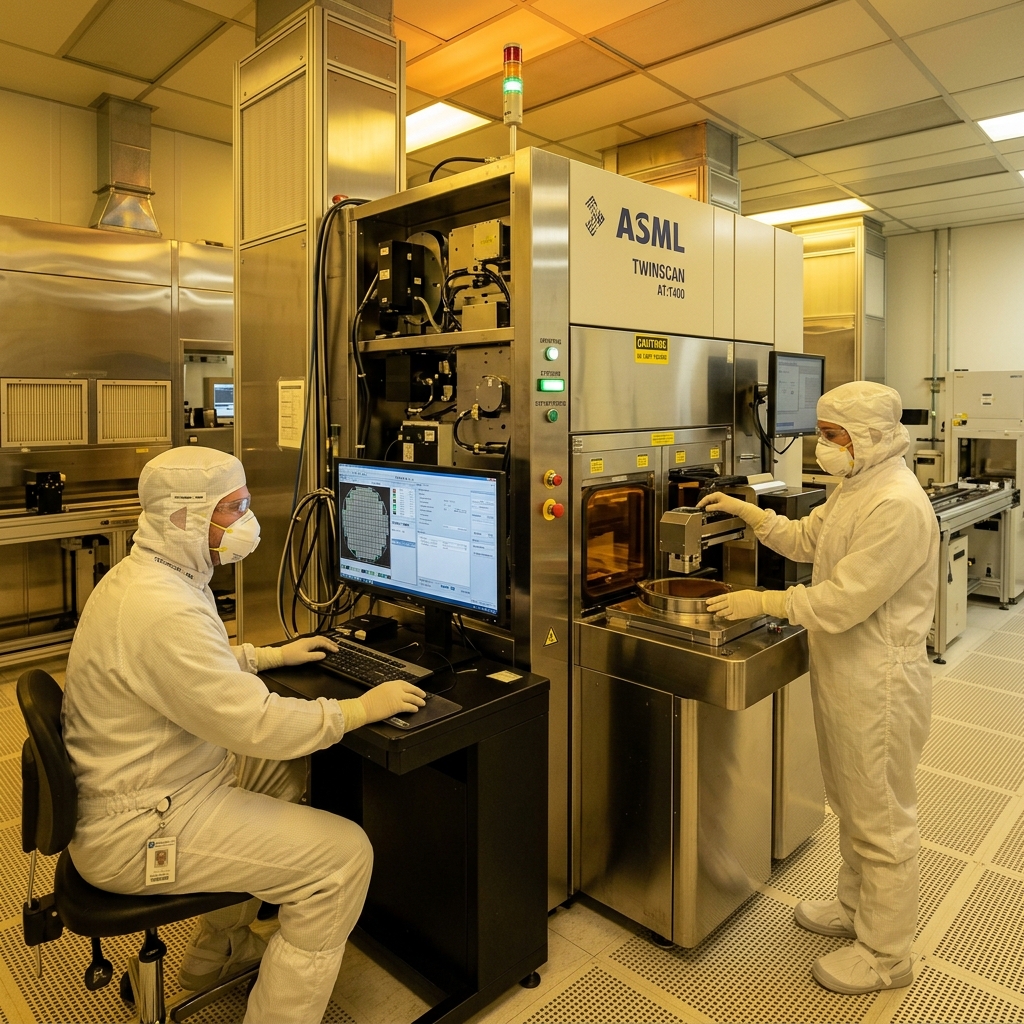
Building cleanroom facilities for advanced packaging is a highly complex engineering challenge. Cleanrooms must maintain extremely low levels of dust and airborne particles to prevent contamination during the micro-assembly process. Even a microscopic speck of dust can ruin a microprocessor, rendering it useless. To achieve this, the facility must install specialized filtration systems, air showers, and automated material handling equipment. This equipment requires precision-machined components that meet strict cleanliness standards, driving demand for domestic CNC machining capacity.
To support this expansion, Arizona has become a major hub for semiconductor companies and suppliers. The state is investing in infrastructure and workforce training programs to support the growing industry. Technical schools are partnering with semiconductor firms to create specialized training courses for technicians. This effort is helping build the skilled workforce needed to operate and maintain the advanced packaging lines. U.S. machine shops are also scaling up their operations to supply the precision tooling and fixtures required by these new cleanrooms.
Why it matters for manufacturers
For electronics manufacturers and aerospace primes, domestic packaging capacity reduces supply chain vulnerability. A secure, onshore pipeline for advanced microprocessors means fewer disruptions from shipping lanes and geopolitical trade tensions. It also speeds up the development cycle for custom silicon designs. When wafers and packaging are located in the same region, engineers can quickly test new chip designs and receive completed prototypes in days, rather than waiting for international shipments.
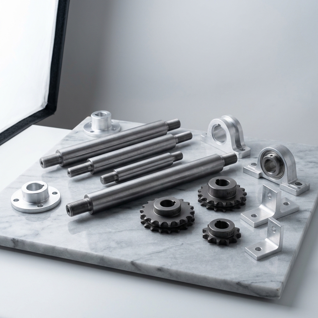
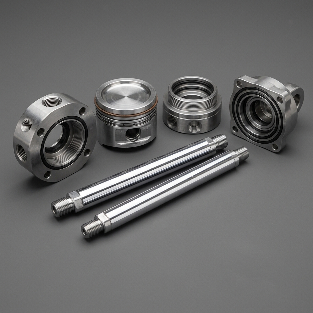
Additionally, building cleanrooms requires highly specialized, precision-machined hardware. From custom vacuum chambers and wafer handling arms to metrology fixtures, components must meet strict cleanliness and tolerance standards. Materials like aluminum and stainless steel must be machined with extremely smooth finishes to prevent particle shedding. Partnering with a CNC machine shop that understands cleanroom requirements is vital. The shop must be able to deliver parts with pristine surfaces and provide special cleaning and packaging services to prevent contamination before installation.
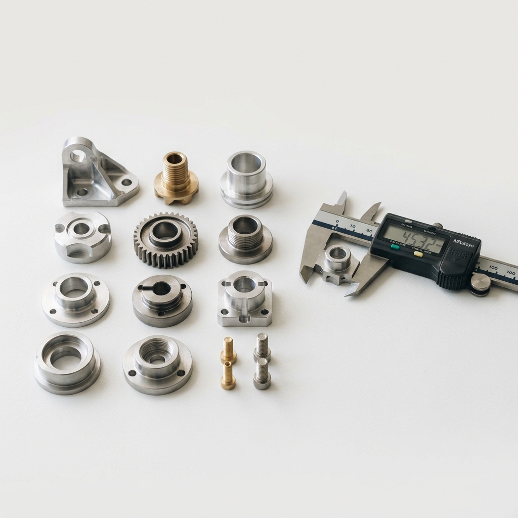
This semiconductor boom is creating major opportunities for domestic machine shops. However, it also requires them to meet higher quality standards. Shops must implement strict quality control processes and invest in high-end CMM equipment to verify part dimensions. They must also manage material traceability carefully, as semiconductor equipment makers require complete certifications for all metals and plastics. Machine shops that can meet these high standards can secure long-term, high-value contracts with semiconductor OEMs, driving steady business growth.
Furthermore, localizing the supply chain helps protect intellectual property (IP). Semiconductor designs are highly proprietary, and sharing files with overseas suppliers increases the risk of IP theft. Working with domestic, ITAR-registered machine shops ensures that sensitive CAD files remain secure. This protection is critical for companies developing advanced processors for defense, aerospace, or proprietary commercial applications. Sourcing locally provides peace of mind and ensures compliance with government security regulations.
What to watch next
Watch for follow-on awards targeting substrate manufacturing. Substrates are the organic or ceramic boards that support the silicon chip and connect it to the main circuit board. Like advanced packaging, substrate production is heavily concentrated in Asia. Without a reliable domestic source of substrates, U.S. packaging plants will still face supply chain risks. The Department of Commerce is expected to announce new grants to expand domestic substrate manufacturing, completing another key piece of the semiconductor supply chain.
We should also monitor the construction progress of TSMC's Phoenix fabs, which are scheduled to begin volume production of advanced wafers over the next 12 months. The success of these fabs will determine the volume of silicon wafers available for domestic packaging facilities. If wafer production ramps up smoothly, it will drive a steady increase in demand for local packaging services, accelerating the growth of the Arizona semiconductor cluster and creating more opportunities for local suppliers.
Finally, watch the labor market in Arizona. The rapid expansion of wafer fabs and packaging plants is creating a huge demand for engineers and technicians. If the state cannot train enough workers, companies may face delays in opening their new facilities. This labor shortage could also push up wages, changing the financial math for future expansions. Workforce development will remain a key focus for both government and industry leaders as they work to build a sustainable domestic semiconductor base.
Additionally, advanced packaging facilities require highly specialized cleanroom tooling and structural support frames. These custom components must be machined to extremely tight tolerances from corrosion-resistant materials like stainless steel and anodized aluminum. Local CNC machine shops play a critical role in supporting these fabs by fabricating custom test fixtures, assembly brackets, and component trays on short lead times. By building a reliable network of domestic machining suppliers, packaging plants can keep their equipment running and adapt quickly to new chip designs, ensuring the overall success of the U.S. semiconductor reshoring effort.
As the Arizona semiconductor cluster matures, packaging facilities will become the focal point of regional supply chain optimization. The proximity of domestic packaging sites to major chip fabs reduces the transit time and logistical complexity of shipping delicate silicon wafers overseas for final assembly. Industry analysts estimate that integrating fabrication and packaging within the same geographic hub can shorten product development cycles by up to thirty percent, providing a significant competitive advantage for American semiconductor suppliers.
Frequently Asked Questions
What is advanced semiconductor packaging?
Advanced packaging is the process of combining multiple silicon dies into a single high-performance processor. This stacking technology is critical for AI and high-performance computing.
Why did the CHIPS Act award $45M to a Phoenix facility?
The grant aims to build domestic packaging capacity. Currently, U.S.-made wafers must be shipped to Asia for packaging. Localizing this step completes the onshore supply chain.
What cleanroom standards are required for chip packaging?
Chip packaging requires cleanrooms that meet strict ISO Class 5 or Class 6 standards to prevent dust contamination from ruining delicate microprocessors.
Why are domestic CNC shops important for the semiconductor industry?
CNC shops machine the custom aluminum vacuum chambers, wafer handling arms, and metrology fixtures required to build cleanrooms and chip fabrication equipment.
Reshoring the wafer fab is only half the battle; without domestic advanced packaging, U.S. chips must still cross the Pacific to be finished.